It is impossible to cover thin film research and technology on a single webpage, but on this page you’ll find some important keywords connected to our division. Use them to explore the fascinating world of thin films. To make it easier we have subdivided them in four groups: thin film technologies, materials, simulations and applications.
Thin film technologies
Thin film technologies are processes to deposit and to change thin layers of materials from a few microns thick down to few atomic layers. Characteristic for thin film deposition is that the growth of the film occurs on a substrate. There are many methods to deposit thin films but our division focuses on vacuum based methods. The methods are based on the production of a vapor. The atoms or molecules of the vapor condense and/or react on the substrate to form the film. Essentially, these methods can be subdivided in two major groups: physical vapor deposition (PVD) and chemical vapor deposition (CVD). When the vapor is produced by a physical method, such as evaporation or sputtering, the technique belongs to the PVD group. Examples are magnetron sputtering, thermal evaporation, pulsed laser deposition to name a few. When the vapor consists of a chemical substance with a low vapor pressure, the deposition method is classified as CVD. Examples are plasma enhanced CVD or atomic layer deposition (ALD). To get a better insight, we highlight a few of the many methods:
- Magnetron sputtering: Magnetron sputter deposition is based on a magnetically enhanced glow discharge. The glow discharge by the application of high voltage between a cathode and an anode. In between both electrodes a gas, typically argon, is present. When the gas discharge is ignited, ions from the gas discharge are accelerated towards the cathode. The ions bombard with high energy the cathode material and as a results atoms from the cathode are ejected. The latter process is known as sputtering which is the physical process to generate a required vapor. Magnetron sputtering is a widely used PVD technique. For example architectural glass is often coated with multilayers to reduce energy losses from building.
- E-beam evaporation:This technique consists of either evaporation or sublimation of certain materials by effect of electron bombardment in a vacuum chamber (typical process pressures between 10-4 and 10-6 mbar). The material to be evaporated/sublimated is located inside a crucible that is grounded. The electrons come from a filament polarized negatively (several kV) located nearby where some electrical current is circulated. The final effect is the heating of the material in the crucible by the electron bombardment. The system is designed in such a way that the material in the crucible either melts and then evaporates, or sublimates directly. This technique is widely used for production of optical coatings and sculptured thin films.
- Atomic layer deposition: Atomic layer deposition (ALD) is a technique for growing thin films for a wide range of applications. ALD is a variant of the chemical vapor deposition (CVD) technique where precursors (gaseous reactants) are introduced into a vacuum chamber to form the desired material via chemical surface reactions. The key difference with other CVD techniques is that technique uses a sequency of gas-phase chemical processes. For example, to deposit aluminium oxide, first trimethyl aluminum (TMA) is introduce to react with the substrate surface by adsorption (chemisorption). If properly designed, this reaction is self-limiting. After removal of the excess of TMA by pumping, water is introduced in the chamber to react with the adsorbed TMA to form Al2O3. Again the reaction is self-limiting, and so after the second step, one monolayer of Al2O3 is formed. Removal of water by pumping prepares the chamber for the next cycle. In this way, layer-per-layer the oxide is deposited, hence the name atomic layer deposition.
Materials
The list of materials which can be deposit as a thin film is endless and includes metals, alloys and compounds. To give you a flavor we discuss in brief a few examples.
- Complex concentrated alloys (CCAs): Where classical alloy design assumed the use of one principle element alloyed with fractions of other elements, this paradigm has changed due to a number of recent discoveries. These show that the combination of several elements in concentrated amounts can lead to combinations of properties that are difficult to obtain with the classical alloy approach. The origin is attributed to synergistic effects between the different elements. CCAs are inherently complex and potentially span a vast composition space, making their
research and discovery challenging. Thin film deposition allow this composition space to be scanned in a combinatorial way. - Magnetic thin films: : Magnetic films are generally composed of transition metals (Fe, Co, and Ni) or alloys based on one or more these elements. The use of thin magnetic films in hard disk and read head application advances the development of information technology, but further developments are still required in order to enhance the performance of volume of information storage, such as heat assisted magnetic recording and microwave-assisted magnetic recording. A rapid growth and promising area is the production of MRAM (magnetic random access memory) with the sandwiched magnetic films as the key materials. The two magnetization states of a spin valve or magnetic tunnel junction are used to encode information. Compared to other technologies currently available based on semiconductor devices, MRAM offers clear benefits: non-volatility, low power consumption, high speed, and high-density storage and irradiation irrelevance. To realize large-scale application of MRAM (including spin-transfer torque MRAM and spin-orbit torque MRAM) in the coming artificial intelligence, big data and computation-in-memory, optimized spin valve or magnetic tunnel junction are still underway, attracting sustained attention both in fundamental research and microelectronics industry. Meanwhile, new methods are emerging for non-volatile memories, such as antiferromagnetic spintronics and topological spin texture (skyrmion), which are based on the antiferromagnetic films and magnetic multilayers with interfacial symmetry broken.
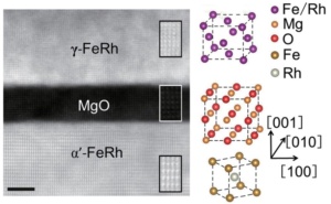
FeRh-based magnetic tunnel junction. - Polymers: As a thin film these material offer innovative solutions for many technological applications such as organic electronics, smart devices for biotechnology, microfluidics, membrane technology, sensors and drug delivery systems. When processed in thin film form their properties can differ from bulk polymers due to the presence of the substrate or the growth conditions. This difference makes these materials also very interesting from a basic science point of view.
- Transparent conductive oxides (TCOs) :This family of materials combine the properties of being transparent in the visible regium of the electromagnetic spectrum while gifted of significant electrical conductivity. In the form of thin films are very important for their use as transparent electrodes, for example to implemented in transparent screens or solar cells. Most popular transparent conductive oxides are Indium Tin oxide (ITO), Aluminium doped Zinc oxide (AZO), or Fluor doped Tin oxide (FTO).

Photo by Kate Trysh on Unsplash - Low and high refractive index materials: Typically, interferometric coatings as those used as antireflective coating in ophthalmic glasses or technical optical elements, or dichroic mirrors and filters, are formed by multilayer stacks of low and high refractive index thin films. Among the most used low refractive index material are SiO2 and MgF2, and as high refractive index are TiO2, ZrO2, Nb2O5, Ta2O5. The desired optical effect is achieved by means of optical design of the multilayer structure (selection of the multilayer architecture as well as the thicknesses and refractive indices of the thin film elements).
Simulations
Models of thin film growth are powerful tools that can help researchers to predict and control the film properties. The evolution of the microstructure, film roughness, and texture can be described by a detailed simulation of the deposition of of atoms/molecules on the surface of the substrate. The first step is an appropriate description of the experimental growth process by the theoretical model. The latter can also be a combination of different models because the processes during thin film growth occur on different time and length scales which can seldom be tackled by one model. Once the model mimics the experimental trends, it provides a wealth of additional information which can assist to control and predict film properties. Indeed, the theory and simulations strategies developed assist in the understanding on how process conditions affect thin film growth. These studies are mostly based on kinetic Monte Carlo, molecular dynamics, or machine-learning approaches, or simulation of the vacuum or plasma conditions under which deposition takes place.
- Kinetic Monte Carlo:The kinetic Monte Carlo (kMC) method simulates the growth as a chain of random events. Each random event depends only on the current state of the system. The random events are for example deposition,adsorption, desorption, diffusion, and chemical reactions. A kMC simulation uses typically an algorithm where at a given time step in the simulation, the set of all possible events and their associated rate constants or “propensities” (i.e., probabilities per unit time) is determined. One of these events is then randomly (hence the name Monte Carlo) chosen to be executed, with the choice weighted according to the propensities of the possible events. To simplify the process of determining the set of possible events, the locations of the particles in the system are usually assumed to be restricted to be at or near the sites of a lattice, and events such as adsorption, diffusion, and so on, are centered near these sites. One can then determine the set of possible events by scanning the lattice and checking what sites are vacant or occupied with particular particle species.
- Molecular dynamics: Molecular dynamics (MD) In this method the physical movements of atoms and molecules are simulated. The atoms and molecules can interact for a well defined period of time. The trajectories of atoms and molecules are calculated by numerically solving Newton’s equations of motion for a system of interacting particles, where forces between the particles and their potential energies are often calculated using interatomic potentials or molecular mechanical force fields.
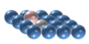
Animation of atomic exchange process involving an adatom on a square surface lattice. Adatom in pink, displaced surface atom in silver for visualization, remaining surface atoms in blue. Credit: Figure taken from Wikimedia Commons (author: Runningamok19)
Applications
The final purpose of the scientific and technological effort to develop thin films with specific characteristics/properties is to implement them in final products and devices to achieve optimized performance towards specific applications. Thin films have a strong impact on our daily life and without exaggeration one can say that technological progress is only possible with the use of thin films. It is hardly impossible to give an overview of all applications of thin films, but one can understand the reason for their widespread application. With a thin film, the surface properties of any solid material can be modified and improved. A few examples are discussed below.
- Protective, hard and tribological coatings: Surface modification is a viable solution to avoid damage under harsh environments, sliding or impacting conditions. Therefore, protective hard tribological films are extensively studied to minimize friction, wear, and degradation of components for numerous applications. Wear could be adhesive, abrasive, erosive, corrosive, due to high-speed particles impacts and to high/low temperature induced chemical interaction with the surrounding environment. Often, hard wear-resistant coatings are carbides, nitrides, carbo-nitrides, borides and oxides grown by Chemical Vapor Deposition (CVD) or Physical Vapor Deposition (PVD) technologies. According to different functional applications, specific properties are required including elemental composition, mechanical properties, microstructure, thickness, adhesion and roughness.
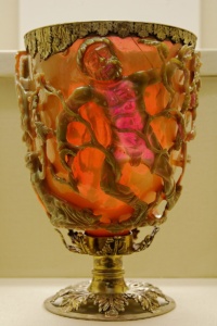
Lycurgus Cup - Plasmonic thin films: The field of nanoplasmonics deals with the study of the electromagnetic phenomena in the nanoscale vicinity of metal surfaces. Although it may sound strange to common sense, the awareness of the resonant properties of plasmonic metal nanoparticles is readily apparent to the naked eye. Because the nanoparticles absorb and scatter visible light, they can generate a wide palette of colors, depending on their concentration, geometries, and dimensions. These optical effects have been used since antiquity (e.g. in ancient Roman glasses (e.g. Lycurgus Cup) and stained-glass windows of medieval cathedrals) and have inspired several practical uses in different scientific and technological areas. The physical interpretation of plasmonic effects only started to gain relevance at the beginning of the 20th century with the theory proposed by Gustav Mie, who deduced a solution of Maxwell’s equations to calculate the extinction spectrum of a metallic nanoparticle in the quasi-static condition. Yet, only in the 1950s it was experimentally demonstrated the existence of self-sustained collective excitations at metal surfaces, which were named thereafter as surface plasmons. About two decades later, in 1974, it was reported for the first time the phenomenon of surface-enhanced Raman scattering (SERS).
- Solar control multilayers: These multilayers have a high transmittance in the visible region
( 380-700~nm), but block the ultraviolet (UV) (10-380 nm) and infrared (IR) (700 nm-1 mm) light. Ideally, the multilayer reflects all UV and IR light, and transmits most of the visible light. The multilayer is generally a sandwich structure of a metal thin film of approximately 10 nm between a pair of dielectric thin films, such as TiO2 or aluminum doped ZnO (AZO), with a thickness of approximately 30 nm. Hence, the following structure is deposited on architectural glazing or on a foil: glass/dielectric/metal/dielectric. Due to its optical properties silver is generally chosen as metal. Non-continuous thin films of other metals (apparent thickness lower than 1 nm) are deposited in between the dielectric thin films and the silver layer, i.e. glass/dielectric/metal/Ag/metal/dielectric to influence the properties of the silver layer, and to protect it during the deposition of the top oxide layer. This type of coatings are for example used to reduce the greenhouse effect and hence to minimize the use of air conditioning.